Atomic (ALD) and molecular (MLD) layer deposition

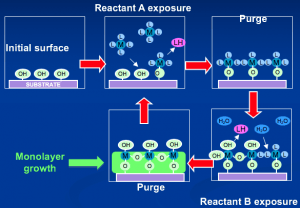
Atomic layer deposition (ALD) relies of self-limiting adsorption/reaction for each precursor to achieve ~single monolayer of each per dose cycle
To create precision 3-D micro- and nano-structures, we rely heavily on conformal materials deposition, often with multiple materials in successive steps. Molecular-scale control of conformal depositions is at the cutting edge in the research community, as well as mainline in semiconductor and related commercial technologies. We partner ALD/MLD techniques with the other tools of microfabrication (etching, patterning) as well as other methods (e.g. nanoporous AAO) to create 3-D scaffolds.
ALD and MLD processes take advantage of selective vapor phase reactions in which a given precursor will adsorb and react on a surface in self-limiting fashion, so that only a monolayer can be added with each exposure cycle. When such self-limiting reaction occurs, thickness control reaches atomic scale while conformality approaches perfection. Accordingly ALD/MLD thickness and conformality control are unmatched, and both properties provide huge benefit to 30D structure fabrication.
We have developed a number of ALD processes for both electrode materials and solid electrolytes, the latter including two versions of LiPON (N-doped Li phosphate). Despite these successes, it should be noted that ALD/MLD processes can be quite complex (e.g., multiple organometallic precursors, imperfect self-limiting behavior, surface nucleation barriers).
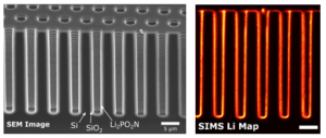
The solid electrolyte ALD processes are having two domains of timely application. First, thin ALD coatings which are ion-permeable offer attractive candidates for electrode protection layers, as we have demonstrated on Li and other reactive metal anodes as well as on conversion materials that undergo profound chemical reactions upon lithiation. Second, ALD solid electrolytes present a major step in the development of a next generation of thin film solid state batteries, where 3D architectures promise higher power-energy performance.
Integrated processing and characterization
Our research methodology is focused on well-controlled multistep synthesis, where sequences of fabrication and characterization steps are carried out under controlled ambient conditions to avoid contamination that would degrade materials and/or distort characterization results. This defines several key elements of our experimental approach, whose combination is unusual.
First, we employ multiple process chambers to enable a variety of ALD/MLD processes, evaporation of normal and alkali/alkaline-earth metals, ion beam etching, and vapor phase plasma etching. Samples can be transported between these process stations under ultraclean conditions, either ultrahigh vacuum or glove box ambient, dramatically suppressing surface contamination and its impact on measured interface and surface properties.
Second, we utilize real-time, in-situ sensing and metrology during the growth of materials. For ALD/MLD, this means spectroscopic ellipsometry and downstream mass spectrometry, so that altered optical properties of the growing thin film and volatile products of the surface reaction are interrogated respectively. We also use the mass spectrometry to monitor volatiles generated during battery cycling as signatures of degradation mechanisms.
Third, we regularly carry out surface analysis using XPS and a variety of related techniques at various stages of nano-/micro- structure synthesis, transporting samples in ultraclean ambient from process to characterization stations. This includes analysis before and after ALD/MLD processes, assessment after a given precursor dose to interrogate the surface chemistry of the ALD/MLD process, and investigations of electrode surface conditions before and after cycling of the electrode in a battery within the glove box.

